A 1,000‑Fold Revolution: Ultra‑Thin Crystal Layers Supercharge Solar Energy
🚀 A 1,000‑Fold Revolution: Ultra‑Thin Crystal Layers Supercharge Solar Energy
A team of scientists at Martin Luther University Halle-Wittenberg in Germany has achieved a groundbreaking leap: an astonishing 1,000‑fold increase in electricity generation from ultra-thin, layered crystals exposed to light. The study, published in Science Advances, focuses on stacking three titanate crystals—barium titanate, strontium titanate, and calcium titanate—to create what they call a “crystal sandwich” absorber. This new design far surpasses the electrical output of pure barium titanate by a striking margin(techspot.com).
🌟 What Are These Materials?
-
Barium titanate (BaTiO₃): A ferroelectric ceramic famed for its ability to generate internal charges when energized by light. It holds a wide bandgap (~3.2 eV), making it less efficient at absorbing sunlight(en.wikipedia.org).
-
Strontium titanate and calcium titanate: Paraelectric materials that don’t naturally separate electric charges but can mimic ferroelectric behavior when combined with others(techspot.com).
Individually, each material performs modestly. But when layered smartly, they reveal extraordinary properties.
⚙️ The "Crystal Sandwich" Breakthrough
Dr. Akash Bhatnagar, the lead researcher, explained the key: alternate a ferroelectric layer with two paraelectric ones. By embedding barium titanate between strontium and calcium titanates, they created an optimized structure capable of capturing more light energy(thebrighterside.news, techspot.com).
This engineered superlattice:
-
Stacks 500 alternating layers, each roughly 200 nanometers thick(pv-magazine.com).
-
Utilizes a high-powered laser deposition technique to vaporize and precisely re-layer the crystals—creating an ultra-thin ~200 nm film with exceptional uniformity(renewableaffairs.com).
💡 Why It Works: Permittivity & Charge Dynamics
The magic lies in the interaction between layers:
-
Permittivity increase: The alternating crystal interfaces boost the material’s ability to polarize, allowing charges to flow more freely under light excitation(techspot.com).
-
Tunable performance: Changing layer thickness adjusts absorption and charge separation—key to customizing electrical output.
In laser testing, the stacked structure produced current levels up to 1,000 times higher than a similar slab of pure barium titanate—even while using two-thirds less of the ferroelectric component(pv-magazine.com).
🧪 Durability Tested: Stability Over Time
Even six months after fabrication, the structure maintained its enhanced current output. This indicates both stability and resilience—critical for real-world applications(impactlab.com).
🌍 Implications for Solar Energy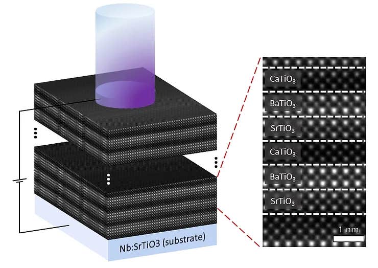
This discovery opens several exciting possibilities:
-
Increased Efficiency
These superlattice absorbers convert light to electricity seamlessly—no need for traditional pn junctions used in silicon photovoltaics—simplifying the manufacturing process(techspot.com, thebrighterside.news). -
Compact Design
Ultra-thin films (~200 nm) outperform thicker pure material layers, saving space and material costs. -
Urban Integration
Smaller, high-output panels can fit roofs and facades in densely populated areas—ideal for city power solutions. -
Simpler Manufacturing
Laser deposition and crystalline stacking are scalable and promise long-lasting devices with less complex packaging than silicon cells.
🔬 Comparing with Silicon and Other Technologies
| Feature | Conventional Silicon | Layered Titanate Superlattice |
|---|---|---|
| Thickness | ~150 µm | ~0.2 µm (200 nm) |
| Junction Required | Yes (p-n) | No |
| Current Output | Standard | ~1,000× barium titanate |
| Manufacturing Complexity | High | Moderate |
| Durability | Proven | Stable over months |
This technology not only challenges silicon but offers unique benefits in simplicity and space usage.
🌐 Scientific and Industrial Outlook
-
Future studies: Researchers aim to fully decode the layer interactions and optimize materials even further.
-
Scaling challenges: Moving from lab to factory-scale continuous layers is the next big engineering hurdle.
-
Material adaptability: Similar strategies may apply to other crystalline combinations, including lead-free perovskites or mixed oxides.
🛣️ Forward Path & Potential
-
Research Roadmap
-
Deep analysis of layer interface physics
-
Testing under various light conditions (sunlight, LEDs)
-
Exploring new crystal pairings
-
-
Prototyping
-
Build small test modules (~cm² scale)
-
Examine integration with glass, metal films, and encapsulation
-
-
Commercial Scale-Up
-
Industrial deposition systems
-
Cost-performance analysis
-
Field testing for durability and real-world efficiency
-
-
Mass Production
-
Integrate with existing solar manufacturing
-
Certification and standards compliance
-
🌈 A Bright Future for Sustainable Energy
This innovative superlattice absorber represents:
-
A new class of ferroelectric photovoltaic technology
-
Potential for ultra-efficient, compact solar systems
-
A simplified alternative to traditional silicon that could lead to affordable, durable, city-compatible solar panels
By reimagining how we layer crystals, scientists are unlocking solar energy potential we've barely tapped into—ushering in a future where every roof, facade, and window could quietly power our world.
🧭 Summary
German scientists have engineered a nanoscale crystal sandwich—alternating barium, strontium, and calcium titanates—to amplify electricity generation from sunlight by 1,000× compared to pure barium titanate(techxplore.com, thebrighterside.news, techspot.com, pv-magazine.com). The structure, deposited with laser precision, remains stable over time and offers a promising, compact alternative to silicon solar cells. While industrial scale-up and deeper mechanistic studies are still needed, this breakthrough presents a notable stride toward simpler, more efficient solar energy systems.


Comments
Post a Comment